NUMERICAL INVESTIGATION OF WAVE EFFECTS IN HIGH-FREQUENCY CAPACITIVELY COUPLED PLASMAS*
Yang Yang** and Mark J. Kushner***
**Department of Electrical and Computer Engineering
Iowa State University, Ames, IA 50010
***Department of Electrical Engineering and Computer Science
University of Michigan, Ann Arbor, MI 48109
1. Introduction
The trend in dielectric etching using capacitively coupled plasmas (CCP) is use of multiple frequencies where a high frequency (tens to hundreds of MHz) dominates ionization and a low frequency (a few to 10s MHz) is used to control ion energy distributions. With an increase in both the high frequency and wafer size, electromagnetic wave effects (i.e., propagation, constructive and destructive interference) can affect the spatial distribution of power deposition and reactive fluxes to the wafer thereby giving rise to limitations on processing uniformity. These effects have been investigated experimentally but are difficult to address computationally in arbitrary geometries due to the coupling between the electromagnetic and the electrostatic fields, the latter of which is responsible for the formation of the sheath.
2. Computational Model
Operating in this high frequency regime is particularly sensitive to the details
of the design of the reactor such as where the rf power is applied and the path
the electromagnetic wave follows from the power cable to the plasma.
To address these issues, a full, time-domain Maxwell equation solver was implemented
into the HPEM with the ability to specify the location that power is fed into the reactor.
The geometry and material properties between the cable and the absorption of that power
in the plasma, in addition to the properties of the plasma itself, then determine the spatial
distribution of the plasma.
In our Maxwell solver, we solve electrostatic (ES) fields and electromagnetic (EM) fields
separately and sum them for plasma transport. For the electromagnetic part, EM fields
launched by power cables are solved using FDTD techniques with Crank-Nicholson scheme
for TM mode propagation. Electrostatic Poisson's equation is solved semi-implicitly to
obtain ES fields generated by charges and DC biases (or any applied DC potential).
With this implementation in the HPEM, multiple frequency CCP tools in the time
domain for arbitrary geometries can be addressed.
3. Results
An example of the consequences of high frequency operation of reactive ion etching (RIE) tools is shown in Figs. 1. Rf powers are fed into the reactor on axis at the top and bottom of the reactor. The top electrode is encased in a dielectric. The bottom electrode is powered at 10 MHz/300 W for this example. A plasma is sustained in Ar/CF4 = 90/10 at 50 mTorr. As the frequency on the top electrode increases from 50 MHz to 150 MHz (Fig. 1), the incident power transitions from being largely electrostatically coupled to being largely electromagnetically coupled. This is manifested by a change in the distribution in power from being edge peaked at low frequencies to being middle peaked at high frequencies.
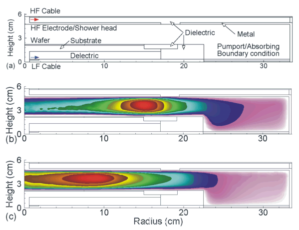 |
| Fig. 1: Modeling of very high frequency CCP tools. (a) Schematic showing the location of the rf power feeds and intervening materials. (b) Electron density for the case with high frequency = 50 MHz/300 W, low frequency (LF) = 10 MHz/300 W, Ar/CF4 = 90/10, 50 mTorr, 400 sccm. (c) HF = 150 MHz. The conditions are otherwise same as those in (b). |
As the power is deposited in a more wave-like manner, there is constructive interference in the center of the reactor, which is responsible for the middle peaked electron density. This transition is evident in there being a radial dependent phase change in the electric field in the sheath of the powered electrode as shown in Fig. 2. The HF field also penetrates the plasma and modulates the LF sheath field, as shown in Fig. 3.
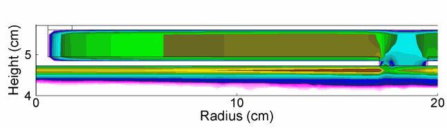 |
| Fig. 2: Axial electric field propagating from the HF power feed to the HF plasma sheath in one LF rf cycle (HF = 150 MHz/300 W, LF = 10 MHz/300 W, Ar/CF4 = 90/10, 50 mTorr, 400 sccm). |
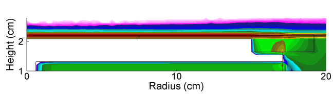 |
| Fig. 3: Axial fields in the LF sheath in one LF rf cycle (HF = 150 MHz/300 W, LF = 10 MHz/300 W, Ar/CF4 = 90/10, 50 mTorr, 400 sccm) |
The impact of changes in HF on the uniformity of ion fluxes and energies delivered to the wafer is shown in Fig.4. With the increasing HF, the plasma becomes non-uniform at 150 MHz and non-uniform ion fluxes onto the wafer results. The spatial plasma non-uniformity also causes radial changes of sheath fields and sheath thickness which eventually translates to the radial non-uniformity of IEADs onto the wafer, as shown in Fig. 4b.
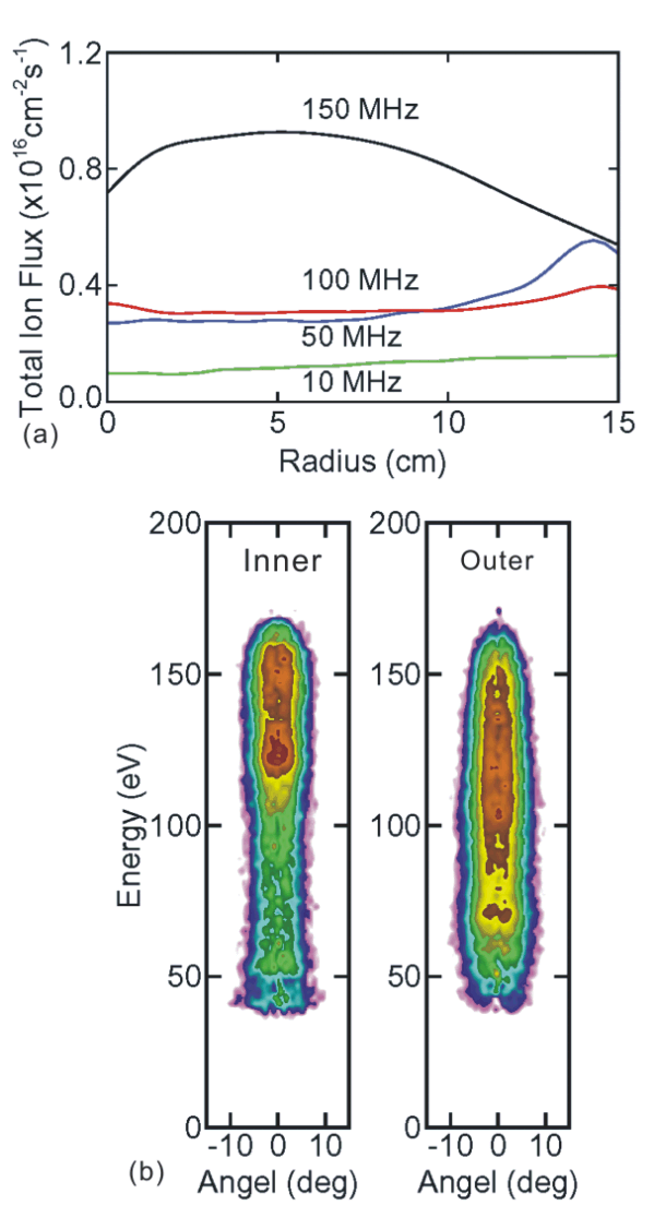 |
| Fig. 4: Distribution of delivered reactant fluxes and energy and angular distributions onto the wafer. (a) Total ion flux incident on the wafer as a function of HF (LF = 10 MHz/300 W, Ar/CF4 = 90/10, 50 mTorr, 400 sccm). (b) Ion energy and angular distributions (IEAD) incident on the inner and outer half of the wafer at HF = 150 MHz. The conditions are otherwise same as those in (a). |
*Work supported by Semiconductor Research Corp., Applied Materials and Tokyo Electron Ltd.
Last updated: Feburary 18, 2009.