Elimination of Twisting in High Aspect Ratio (HAR) SiO2 Etching in Fluorocarbon Plasmas---
High Energy Electron (HEE) Effects*
Mingmei Wang** and Mark J. Kushner***
**Department of Chemical & Biological Engineering
Iowa State University, Ames, IA 50010
***Department of Electrical Engineering & Computer Science
University of Michigan, Ann Arbor, MI 48109
1. Introduction
Twisting is an important issue in optimizing HAR (>10) sub-micron to nano-scale features. Twisting is the random deviation from the vertical of features. There are three dominant causes for twisting. The first results from the non-uniformity of macro-scale inputs, such as ion and neutral energy angular distributions and fluxes, which could be effectively controlled by modulating reactor parameters (e.g., pressure, bias power, and frequency). The second cause for twisting comes from the shrinking size of feature openings to the plasma. When etching features with an open area of only 100s nm2, the time interval between two incoming particles could be as long as 100s ns. This leads to feature-to-feature variations and, if the random sequence of reactants is non-uniform, may produce asymmetric profile especially for polymer-based dielectric etching processes. The third is the consequence of charging. Non-uniform electric fields formed in the feature due to stochastic charging of sidewalls and charge trapped in polymers decelerate (or accelerate) incident ions and may deviate their trajectories from vertical. Intra electric field buildup due to ion bombarding increases with increasing aspect ratio of features. Producing or injecting a narrow angle spread high energy electron (HEE) flux into the feature may be an effective way to neutralize positive charges accumulated during etching. Twisting was investigated using reactor and features scale models. The 2-dimensional Hybrid Plasma Equipment Model (HPEM) was used for reactor scale simulation. The fluxes of reactant species and their energy and angular distributions from the HPEM were then input into the Monte Carlo Feature Profile Model (MCFPM), where the surface (e.g., mask, PR, semiconductors) of the wafer was resolved using a two-dimensional rectilinear mesh. Poisson's equation was solved to obtain charge induced potentials and electric fields in the feature.
2. Elimination of Twisting
Results are discussed from a computational study of a dc augmented capacitively coupeld plasma (CCP) for etching HAR features in SiO2 over Si in Ar/C4F8/O2 plasma. An rf bias (10 MHz) was used to control the energy and angular distribution of reactive ions. And a dc electrode on the top was used to produce HEE beams. The cylindrically symmetric CCP reactor is schematically shown in Fig.1. The base case operating conditions are Ar/C4F8/O2=80/15/5 at 40 mTorr with a flow rate of 300 sccm. The substrate delivers a power of 1 kW by adjusting voltage. A negative dc bias is externally applied to the upper electrode and its value is adjusted to deliver a power of 200 W.
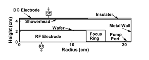 |
| Fig. 1: Schematic of dc augmented single frequency CCP reactor. |
The rf cycle averaged electron density, total ion density and power deposition density are shown in Fig.2. The rf voltage to deliver 1 kW is 1047 V with a self generated dc bias of -644 V. The applied dc bias on the upper electrode to deliver 200W is -430V. Both the electron density and total ion density have edge-peaked distributions. This results partly from a low frequency of 10 MHz and the incident power being largely electrostatic coupled. The low aspect ratio of the reactor could also lead to this edged peak in ion density. The electron density is peaked at 2.0x1010 cm-3, which is typical in a CCP reactor as shown in Fig.2a, and the ion density has a maximum value of 3.8x1011 cm-3 (Fig.2b) indicating an electronegativity of about 20. Fig.2c shows a fairly uniform power deposition along the surface of both electrodes with a peak value of 2.7 W/cm3.
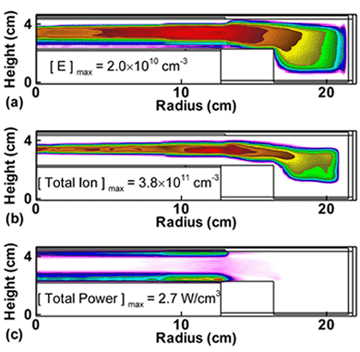 |
| Fig. 2: Bulk plasma properties for the base case. (a) Electron density; (b) Total ion density; (c) Power deposition density. The maximum value in each frame is noted. |
The plasma potential at 3 kW as a function of height during the rf cycle is shown in Fig.3. On the top electrode, a negative -270 V dc voltage was applied to deliver a power of 200 W. This negative potential attracts ions from bulk plasma to strike the surface of the top electrode where a high energy secondary electron beam is emitted. The high voltage (1215V, with -203V dc bias) of the rf bias generates a thick sheath above the wafer in which ions are accelerated.
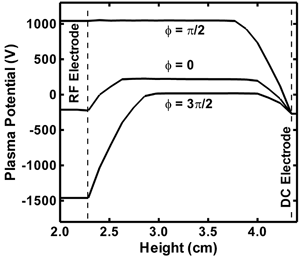 |
| Fig. 3: Plasma potential as a function of chamber height and phase at rf 3kW. |
A set of 21 cases with different random seeds in the MCFPM was used to simulate trenches with a mesh resolution of 3 angstrom which is comparable to an atom's size. Each trench has a 12 nm thick hard mask and a 6 nm opening to the plasma with etching depth of around 150 nm (aspect ratio = 25). 5 profiles selected from the 21 trenches are shown in Fig.4. 3 trenches in 21 twist in profile similar to that shown in the 4th trench in Fig.4a. If including HEE beams in the model, as shown in Fig.4b, twisting is effectively eliminated in all cases, although the features have statistical variationst due to the very small size of the trenches. Since HEE beams neutralize positive charge deep into the trench, interior electric fields which deflect ions are decreases. The etch rate is slightly increased on average for the cases with HEE beam fluxes.
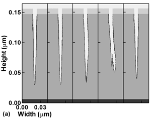 | 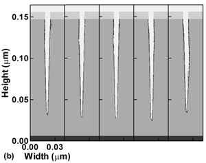 |
| Fig. 4: Atomic scale simulation of HEE beam effects on eliminating profile twisting with hard mask on top of features. (a) Etching profiles without considering HEE species; (b) Etching profiles with HEE species in chemistry. Mesh resolution = 3 angstrom, AR = 25, Prf = 1kW. |
To investigate how dc augmentation affects HEE energy angular distribution and fluxes, four dc voltages (0 V, 400 V, 500 V, 750 V) were simulated in the CCP reactor. The rf bias voltage was kept constant to get similar ion energy and angular distributions as shown in Fig.5a. The energy angular distribution of HEE beams corresponding to different dc voltages are shown in Fig.5b. The HEE flux increases with increasing dc voltage. Note that HEE beams will be naturally produced in CCPs due to the oscillation of the plasma potential (Vdc = 0 V). The use of dc augmentation is a means to control the extent of the energy and the flux of electrons.
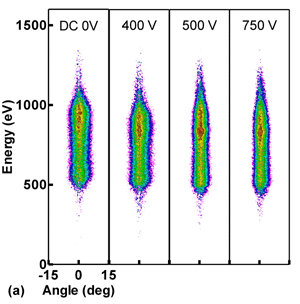 | 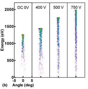 |
| Fig. 5: Dc voltage effects on HEE beam energy and angle distributions and fluxes. (a) ion energy and angular distributions at four dc voltages (0 V, 400 V, 500 V, and 750 V); (b) HEE energy and angular distributions at the four dc voltages; (c) HEE fluxes at the four dc voltages. Rf bias voltage remains constant (1500 V) to ensure getting similar energy and angle distributions and fluxes for ions as shown in (a). |
21 trenches with different random seeds were simulated using input parameters from four different dc voltages (0 V, 400 V, 500 V, 750V) respectively. Fig.6a and Fig.6b show two typical sets of profiles selected from the 21 cases. Without dc augmentation (Vdc = 0 V), there are 7 trenches twisted out of 21 cases. When the dc voltage increases to 400 V or 500 V, the number of twisting profiles is decreased to 5. While for cases with a dc voltage 750 V, the fraction of twisting is only 3/21. Thus increasing dc voltage is demonstrated having the capability to eliminate twisting statistically.
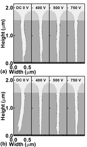 |
| Fig. 6: Statistical feature profile prediction at different dc voltages. (a) Typical profiles with random number seed 1 selected from 21 cases at four different dc voltages (0 V, 400 V, 500 V, and 750 V); (b) Typical profiles with random number seed 2 selected from 21 cases at the four different dc voltages. Mesh resolution = 5 nm, AR = 20, rf 4 kW. Twisting probability of the 21 cases at the three dc voltages are: 7/21 at Vdc = 0 V, 5/21 at Vdc = 400 V, 5/21 at Vdc = 500 V, and 3/21 at Vdc = 750 V. |
*This work was supported by Semiconductor Research Corp., Micron Corp. and Tokyo Electron Ltd.
Last updated: February 18, 2009.