The Charging Process of Rollers in Print Engines with Atmospheric Pressure Plasmas*
1. Introduction
A conductive charge roller (CR) is an important component of electrophotographic (EP) printing technologies to uniformly charge the surface of a photoconductor (PC) or paper to form an image pattern. A typical CR is biased with a dc, pulsed dc or ac voltage up to a few kV. A microplasma is then produced in the small gap of the converging CR and PC, and charges the PC surface. This reduces the voltage drop across the gap which then terminates the discharge. In the printing process, this underlying surface is continuously moving during charging, and a periodic charging pattern is sometimes produced. (See Fig. 1.) These issues have been computationally investigated in this study.
a)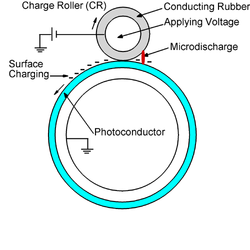
|
b)
|
Figure 1. Surface charging of a photoconductor (PC) by a conductive roller (CR). (a) Schematic of cylinder CR and PC and (b) Periodic charging pattern. |
|
2. Description of the Model and Conditions
The modeling platform used in this investigation, nonPDPSIM, is a first principles, two-dimensional and multi-fluid hydrodynamics simulation performed on an unstructured mesh. nonPDPSIM solves transport equations for charged and neutral species, Poisson's equation for the electric potential and the electron energy conservation equation for the electron temperature. A Monte Carlo simulation is used to track sheath accelerated secondary electrons emitted from surfaces. Rate coefficients and transport coefficients for the bulk plasma are obtained from local solution of Boltzmann's equation for the electron energy distribution. Radiation transport is addressed using Green's function approach. The model geometry is shown in Fig. 2a. A conducting rubber cathode cylinder is biased to -3 kV, and the opposing cylindrical electrode is covered with a dielectric photoconductor. The discharge is initiated with current of 10-3 A-cm-2 for 10 ns. The gap is filled with 1 atm dry air at 300 K.
3. Charging Process of the Roller
The electron density, electron impact ionization source from bulk electrons (Se), ionization by the secondary electron beam (Ssec) and photoionization (Sphoto) are shown in Fig. 2b. After an avalanche occurs adjacent to the electron emission point, a streamer is initiated and propagates towards the underlying PC. Meanwhile, laterally propagating electrons and secondary electrons help trigger an avalanche at smaller gaps having a higher E/N. A locally enhanced electric field at the edge of the spreading plasma then produces a cathode directed secondary discharge. The streamer spreads on the PC, reduces the voltage drop and then terminates the discharge. During the charging process, electron impact ionization sources from bulk plasma electrons and sheath accelerated secondary electrons are comparable, while photoionization is insignificant. Having said that, photoemission from the CR surface provides remote seed electrons which triggers avalanche.
a)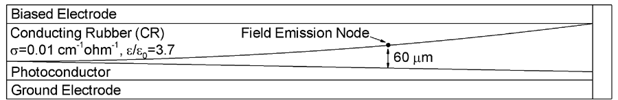
|
b)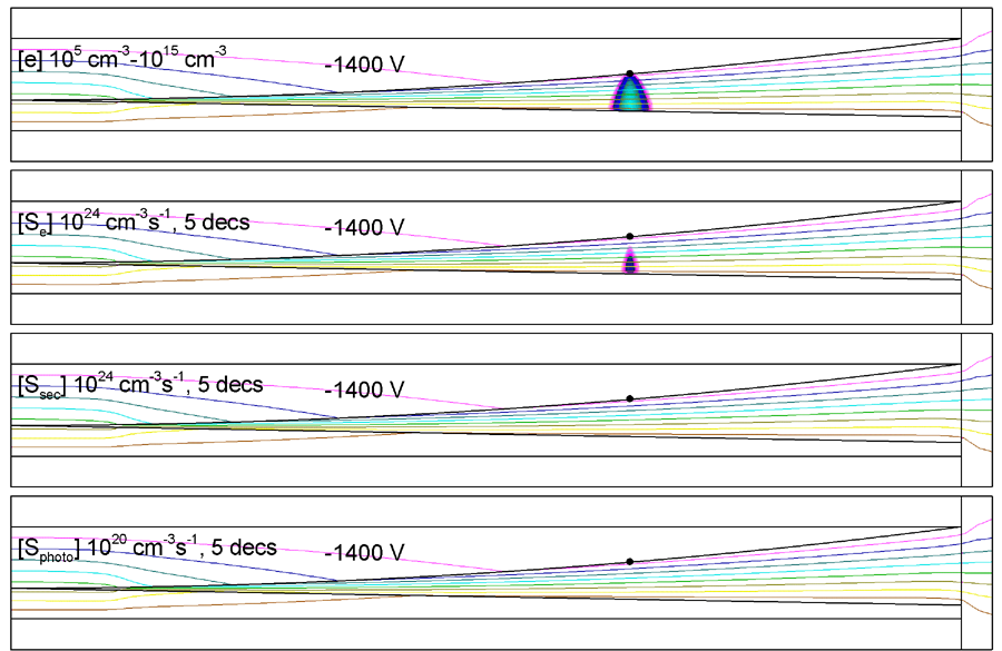
|
Figure 2. Charging process of a conductive roller. (a) Model geometry of cylinder CR and PC and (b) plasma parameters for microplasma in CR in print engine (electron density [e], electron impact ionization source and potential contour lines). |
4. Location Matters: Current Emission from Different Locations
The location of the initial electron emission can significantly change the plasma dynamics and charging properties. Results from the simulation for microplasmas initiated by current emission at 85μm, 135μm and 177μm gaps are shown in Fig. 3. When the emission occurs at a smaller gap (85 μm), an electron avalanche occurs at the emission point which then produces a streamer propagating towards the underlying PC and which charges it. Cathode directed secondary discharges are produced by laterally propagating electrons and secondary electrons. When a current is emitted at 135μm gap, electron avalanche occurs at a location closer to the contact point of the CR and PC and is triggered by laterally propagating and secondary electrons. No electron avalanche occurs when field emission occurs at a 177μm gap where the local electric field is below the critical E/N. Diffusion and photoionization are unable to seed the avalanche.
a)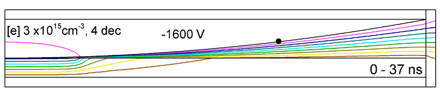
|
b)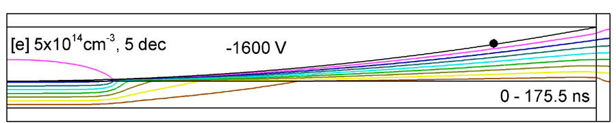
|
c)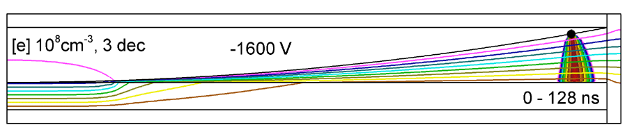
|
Figure 3. Microdischarge initiated by field emission occurs at (a) 85μm (b) 135μm and (c) 177μm. |
5. Moving Photoconductor
In reality, both the CR and PC rotate during the charging process in EP printing. The voltage on the CR remains constant if the its conductivity is sufficiently high. For a stationary CR and PC, surface charging on the PC reduces the local electric field and eventually terminates the discharges. In the case of a moving PC surface, as the underlying PC surface translates (in this case to the left), surface charges are also translated while the incoming surface is uncharged. The uncharged surface restores the local E/N, and electron avalanches occurs. The simulation results of relatively slow and rapid moving surface are shown in Fig. 4. The moving PC surface continually brings uncharged surface towards the left. When the voltage drop between CR and uncharged PC surface rebounds, an electron avalanche occurs, and microdischarge re-ignites. The re-ignition process then forms a periodic charging pattern on the PC surface.
a)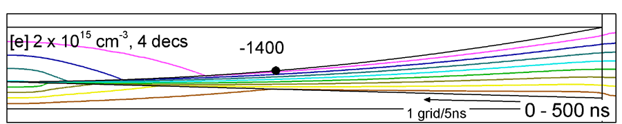
|
b)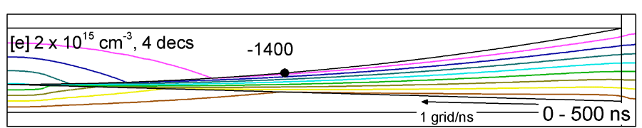
|
Figure 4. Discharge sustained between conductive CR and (a) slowly and (b) rapidly moving PC surface. |